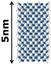
The continued downscaling of transistors reaches around 10 nanometers in the near future. Researchers from DTU Nanotech pursue even smaller devices - going towards 5 nm corresponding roughly to a few hundred atoms in length.
A transistor is the fundamental component of modern electronic devices. The development towards smaller or more multi-functional electronic devices demands for a reduction in the size of the building blocks, such as transistors, used to construct the devices.
Every atom matters
Besides posing challenges to the fabrication process of still smaller transistors, the downscaling requires that researchers consider more seriously the regime where "every atom matters" (Fig 1a). The heat-release (Joule heating) in the smaller volumes and the fact that the electrons inside the device are quantum waves with a wavelength comparable to the device size pose technological challenges for the industry. Furthermore, to control the electrical properties of the semiconductor, dopants, i.e. tiny impurities, are added to the semiconductor material.
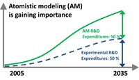
Professor Mads Brandbyge says that "simulation and computation are important when we develop and design today's electronics - and they will be even more important in the future" (Fig 1b). Wider choice of materials is needed as well as new device structures. New physical models, computational methods, and software using atomistic descriptions (that is, descriptions relating to atoms) are in demand. The tools of today, such as the so-called Technology Computer Aided Design tools, TCAD, do not take into account the nanoscale dimensions of the device and therefore alternatives need to be developed.
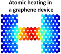
Fig 1. (a) Size of 5nm piece of Silicon - note the atoms! (b) The gain of importance of modelling versus experimental research (courtesy of QuantumWise A/S). (c) Calculated current-induced heating of a nanoconstriction in graphene.
For a long time, researchers at DTU Nanotech have developed methods and software tools which can be used in the search for new nanoelectronic devices.
Collaboration project
In a collaboration project with QuantumWise A/S and DTU Compute, researchers from DTU Nanotech work to include the Joule heating and heat transport in the atomistic device simulations. Professor Mads Brandbyge says that "we need accurate atomistic calculations to get input parameters for higher-level TCAD simulations of e.g. the Joule heating in the still smaller transistors".
The researchers have developed methods and software tools that are now being tested before release. The preliminary results were presented at the SISPAD (Simulation of Semiconductor Processes and Devices) 2015 international conference in September. Postdoc Tue Gunst explains that "our results illustrate the predictive capabilities of nanoscale simulations, when it comes to material parameters and heating of novel devices". A few examples are the characterisation of electrons' ability to move around in devices (the so-called mobility) made from emerging two-dimensional materials and the heating of nanostructured graphene (see Fig 1c).
The collaboration project was funded in 2013 by the Danish National Advanced Technology Foundation.
Story Source:
The above story is reprinted with permission of Technology.


